Bridging academia and industry since 20042004年から、大学と産業の架け橋に
A research-driven venture enterprise originating from Shizuoka University, dedicated to thin-film technology for clean energy. 静岡大学発の研究開発型ベンチャー企業として、クリーンエネルギーのための薄膜技術に取り組んでいます。
Our story創業の経緯
In 1989, seeing great promise in terms of energy saving, resource saving and low cost, I began researching spray pyrolysis deposition (SPD). With simple equipment and easy operation, this method forms thin films in open air in a short time through thermal decomposition and chemical reaction of raw materials. Our first hand-made apparatus evolved within a few years into large, automated systems.
In 2004 I founded SPD Laboratory with the goal of spreading the practical applications of the SPD thin-film technology I had developed at Shizuoka University. Bridging the gap between academia and industry with creative, tailor-made products has been our target from the beginning. We produce SPD machines and build the latest dye-sensitized and perovskite solar cell systems using thin films prepared by SPD — aiming always to supply products of the highest quality at a good price.
1989年、省エネ・省資源・低コストの観点から将来性を感じてスプレー熱分解法(Spray Pyrolysis Deposition)の研究に着手しました。この方法によれば、簡単な装置と容易な操作で、大気中で原料の熱分解・化学反応による物質変化を伴って薄膜を短時間に形成できます。当初の手作り装置から、数年後には自動化した大型装置へと進化させました。
2004年、SPD薄膜形成技術の発展と普及を目指してベンチャー企業をスタートさせ、SPD装置および透明導電膜(FTO/ITO)の製造販売、色素増感太陽電池(DSC)・ペロブスカイト太陽電池(PSC)など次世代太陽電池の研究開発、SPD技術に関する調査研究・受託研究を事業内容とする研究開発型企業を目指しています。
Mission, philosophy and direction理念と事業の方向性
Mission使命
As a venture enterprise originating from Shizuoka University, we aim to introduce next-generation technology to people all over the world and make their lives more comfortable by applying our accumulated intellectual property to clean energy supply and environmental preservation.
静岡大学発のベンチャー企業として、蓄積した知的財産をクリーンエネルギーの供給と環境保全の課題解決に生かし、次世代の技術を世界中の人々に届け、より快適な暮らしの実現を目指します。
Philosophy企業理念
In the fields of energy and the environment, we take on the challenge of creating creative, high-value-added products that meet real needs — contributing to our customers and to society.
私たちはエネルギーと環境の分野において、ニーズに合った創造的で付加価値の高い製品づくりに挑戦して、顧客にも、社会にも貢献します。
Customer-oriented & tailor-madeCustomer-oriented & Tailor-made
Every product is developed from a researcher’s point of view, so we are confident in its precision and ease of use. Through an “open lab” approach and close collaboration with universities and institutes in Japan and abroad, we keep expanding our line-up to meet customer needs.
弊社製品はすべて研究者目線で開発されるのが特徴であり、機能の的確さと使い勝手の良さには自信があります。オープンラボを心がけて国内外の大学・研究所と連携を図り、お客様のご要望に応えて製品の種類を増やしてきました。
Business status and outlook事業の状況と展開
In June 2019 we celebrated our 15th anniversary. Building on our experience with SPD technology and dye-sensitized solar cell manufacturing, we are committed to: (1) being unique and number one in processes, materials and instruments; (2) thoroughly pursuing “High Quality – Best Price”; and (3) supporting young researchers. True to our venture spirit — “rich in ideas; perseverance is power” — we will continue to be of service to you.
Our main products fall into four groups: thin-film deposition equipment, next-generation solar cell (DSC/PSC) fabrication processes, solar cell performance evaluation systems, and supercapacitor/battery evaluation systems. The spread of photovoltaics requires integration with power storage devices, and we are focusing our thin-film expertise on this area too.
2019年6月、お蔭様で創業15周年を迎えると共に、創業以来のSPD技術と色素増感太陽電池製造を中心にした弊社の事業展開に変化が生じてきました。これまでの経験と実績に基づいて、(1) プロセス、材料、機器装置のすべてにおいて、ユニークでナンバーワンを一段と目指す、(2) 経営改善に向けて、High Quality - Best Priceの徹底、(3) 若い研究者への協力と支援などに取り組もうとしています。ベンチャー企業として培ってきた「アイディア豊かに、継続は力なり」の信念で、益々存在感を高めて皆様のお役に立つ所存です。
主な製品は薄膜製造装置、次世代太陽電池(DSC/PSC)製造プロセス、太陽電池性能評価システム、スーパーキャパシタ/バッテリー評価システムのグループに大別されます。今後の太陽光発電の普及と発展には電力貯蔵デバイスとのシステム化が必須であり、弊社はこの面の研究開発にも薄膜技術を通じて注力します。
Business policy今後の事業方針
- Manufacture and sale of SPD thin-film deposition systems, DSC and PSC prototyping equipment, and FTO / ITO transparent conductive films
- Manufacture and sale of new solar cell performance evaluation systems
- Contract prototyping and research on next-generation thin-film solar cells
- Development of thin-film power storage devices
- Prototyping of thin-film devices and development of their evaluation equipment
- SPD薄膜形成装置、DSC及びPSC試作装置、FTO/ITO透明導電膜の製造販売
- 新規太陽電池性能評価システムの製造販売
- 次世代薄膜太陽電池に関する試作・調査研究の受託
- 薄膜電力貯蔵装置の開発
- 薄膜応用デバイスの試作とその評価装置の開発
What is Spray Pyrolysis Deposition?SPD(スプレー熱分解法)とは
SPD is one of the chemical thin-film formation methods: a solid film is deposited from a liquid phase sprayed onto a heated substrate. 化学的製膜法のひとつであるSpray Pyrolysis Depositionの略称で、加熱基板上に噴霧された液相から固相を析出し、薄膜として堆積させる方法です。
1. Principle1. 原理
SPD is performed at atmospheric pressure using a simple apparatus consisting of an atomizer, air compressor, solution reservoir and heater (Fig. 1). The raw-material solution is atomized onto a heated substrate by a pneumatic system — intermittently rather than continuously, to keep the substrate temperature constant, since the mixture of solution and air cools the substrate. Inorganic and organic metal compounds are used as raw materials; the principal components and composition of the starting solution are retained in the deposited film (except for easily evaporated additives), so the method normally gives the prescribed film composition.
SPDは、噴霧器、エアコンプレッサー、溶液タンク、ヒーターからなる簡単な装置を用い、大気圧下で行います(図1)。原料溶液は空圧システムにより加熱基板へ向けて噴霧されます。溶液と空気の混合物は基板温度を低下させるため、連続ではなく間欠的に噴霧して基板温度を一定に保ちます。原料には無機・有機の金属化合物が幅広く使用でき、揮発しやすい添加物を除き、出発溶液の主成分と組成がそのまま膜に保持されるため、通常は所定の成分・組成の膜が得られます。
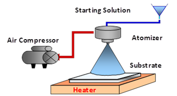
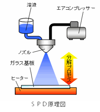
Fig. 1. Schematic diagram of an SPD apparatus図1. SPD装置の原理図
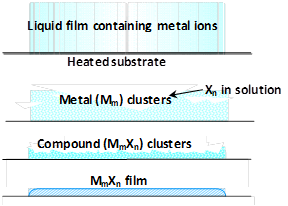
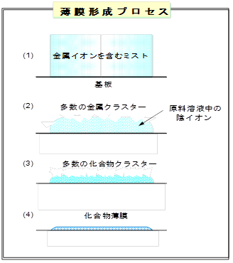
Fig. 2. Film deposition process図2. 薄膜形成プロセス
2. Deposition process2. 製膜プロセス
- Countless mists from the atomizer wet the substrate and form a liquid film. According to Gibbs’ phase rule, the solvent stays at its boiling temperature until fully evaporated, even though the substrate is much hotter.
- The temperature of the remaining solute rises rapidly, yielding metal clusters through thermal decomposition and/or chemical reaction.
- These metal clusters are instantly converted to compound clusters by reacting with negative ions in the solution.
- Condensation and cohesion of the compound clusters on the substrate immediately yield a solid film.
- 加熱された基板に向けて原料溶液を噴霧すると、無数の微小液滴が基板を濡らして液膜を形成します。基板温度が溶媒の沸点よりはるかに高くても、ギブズの相律により溶媒は完全に蒸発するまで沸点に保たれます。
- 溶媒の蒸発後、残った溶質の温度が急上昇し、熱分解・化学反応によって金属クラスターが生成します。
- 金属クラスターは溶液中の陰イオンと反応し、瞬時に化合物クラスターへと変化します。
- 化合物クラスターが基板表面で凝縮・凝集し、直ちに固体の薄膜が形成されます。
3. Features3. 特徴
SPD produces dense, even films with thicknesses from 10 nm to 10 µm. Complex-compound and solid-solution films can also be obtained as non-equilibrium or metastable phases by controlling starting solutions and substrate temperatures. Particle shape and size, microstructure and texture are controllable through deposition conditions. Film thickness increases in proportion to solution concentration, spray rate, time and number of cycles, and depends on substrate temperature, solute vapor pressure and wetting ability. Pausing the atomization to avoid cooling the substrate is believed to promote atomic diffusion, crystallization of fine particles and densification — contributing to film quality.
SPDは溶液から膜厚10 nm~10 µmの緻密で均一な薄膜を形成できます。出発溶液と基板温度の制御により、非平衡相・準安定相として複合化合物や固溶体の膜も得られます。多結晶膜の粒子の形状・大きさ、微細構造や組織は製膜条件によって制御可能です。膜厚は溶液濃度、噴霧速度、噴霧時間、サイクル数に比例して増加し、基板温度、溶質の蒸気圧、溶液の濡れ性にも影響されます。基板温度の低下を避けるための噴霧休止中に原子の拡散・移動が起こり、微粒子の結晶化と組織の緻密化が進むと考えられており、これが膜質の向上に寄与しています。
Advantages of SPDSPDのメリット
- Simple apparatus and easy operation装置が簡単、操作も容易
- Film formation possible in open air大気中で製膜可能
- Wide choice of raw materials原料の選択幅が広い
- Easy adjustment of components and composition成分・組成の調整が容易
- Low-temperature formation possible低温形成が可能
- High deposition rate製膜速度が高い
- Easy scale-up to large areas and coating of complex shapes大面積化が容易、複雑形状物へのコーティングも可能
Promising future developments今後の展開
Transparent conductive oxide (TCO) films透明導電膜(TCO)の製造販売
Using SPD we prepare fluorine-doped tin oxide (FTO) and tin-doped indium oxide (ITO) films on glass with high electrical conductivity and visible-light transmittance, for display panels, electromagnetic-shielding glass, solar cells and more.
SPD法により、高い導電性と可視光透過率を持つフッ素ドープ酸化スズ(FTO)およびスズドープ酸化インジウム(ITO)薄膜をガラス上に形成します。ディスプレイパネル、電磁波シールドガラス、太陽電池などに利用できます。
Coated substrates & patterned filmsコーティング基板・パターン製膜R&D on DSC and PSCDSC・PSCの研究開発
A DSC consists of a photo-electrode coated with a porous wide-band-gap semiconductor and dye, and a counter electrode coated with a very thin platinum layer, with electrolyte in between. Requiring no vacuum system and no hazardous materials, DSCs are an attractive low-cost next-generation solar cell — switching can save more than 50 % of the cost.
DSCは、色素を吸着させたワイドバンドギャップ半導体の多孔質層を持つ光電極と、極薄の白金層を持つ対極の間に電解液を満たした構造です。真空装置や有害物質を必要とせず低コストで製造できるため、高価なシリコン太陽電池に代わる次世代太陽電池として有望で、50 %以上のコスト削減が可能です。
DSC fabrication equipmentDSC製造装置Instrumentation for solar cells & power storage太陽電池と蓄電のための計測技術
We aim to combine DSC/PSC photovoltaics with battery/supercapacitor power storage. We have initiated PSC processing with piezoelectric inkjet printing and developed PV power analyzers with MPPT — contributing to next-generation solar cell research together with highly motivated scientists and engineers.
DSC/PSCによる太陽光発電と、バッテリー/スーパーキャパシタによる蓄電を組み合わせたシステムの実現を目指しています。ピエゾ式インクジェット印刷によるPSC作製プロセスや、MPPT機能付きPVパワーアナライザーの開発に取り組み、意欲ある研究者・技術者との協力を通じて次世代太陽電池研究に貢献していきます。
Characterization instruments太陽電池評価装置At a glance会社概要
| Company name社名 | SPD Laboratory, Inc.株式会社SPD研究所 |
|---|---|
| Established設立 | June 1, 20042004年6月1日 |
| Representative代表者 | Shoji Kaneko, Ph.D., President & CEO代表取締役 金子正治(工学博士) |
| Address所在地 | 2-35-1 Johoku, Chuo-ku, Hamamatsu, Shizuoka 432-8011, Japan〒432-8011 静岡県浜松市中央区城北2-35-1 |
| Phone / Fax電話/FAX | +81-53-474-7901 / +81-53-401-7080 |
| Emailメール | inq@spd-lab.com |
| Business事業内容 | Manufacture and sale of SPD thin-film deposition systems, solar cell evaluation instruments, DSC/PSC fabrication equipment and TCO films; contract research on SPD technology and next-generation solar cellsSPD薄膜形成装置、太陽電池評価装置、DSC/PSC製造装置、透明導電膜の製造販売。SPD技術および次世代太陽電池に関する調査研究・受託研究 |