|
Description |
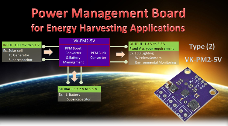
The circuit board is designed to collect and manage microwatt (μW) to milliwatt (mW) power generated from various DC sources such as solar cells or thermoelectric generators. In addition to the highly efficient boosting charger, this board includes a highly efficient, nano- power buck converter in the output stage. A supercapacitor (0.22F 5.5V) is installed onboard as a storage.
|
Characteristic
|
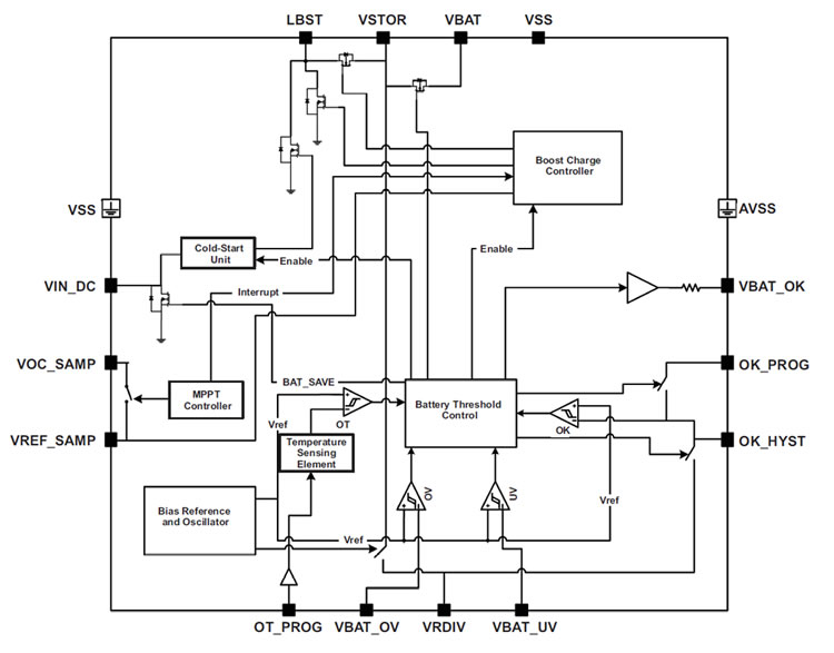
- Ultra Low Power, High Efficiency DC-DC Boost Converter/Charger
- Programmable step down regulated output Buck Converter
- Continuous energy harvesting from low voltage input supply: VIN ≥ 100 mV
- Full operating quiescent current: 488 nA (typical)
- Cold start voltage: VIN ≥ 600mV (typical)
- Programmable Dynamic Maximum Power Point Tracking (MPPT)
|
Energy source input voltage |
0.1V – 5.1V (Cold start voltage is 600 mV)
It will continue energy harvesting from VIN as low as 100 mV
|
Energy storage component and Voltage |
0.22 F, 5 V Supercapacitor mounted onboard
Energy can be stored to rechargeable li-ion battery, thin-film battery, super-capacitor, or conventional capacitor. Voltage range is 1.3 V - 5.3 V (Can be set to your voltage requirement)
|
Working environment temperature |
-40 ~85 ˚
|
Switching frequency
|
Boost charger up to 1MHZ, Buck converter up to 500 kHz
|
Working mode |
Cold start mode, boost mode, thermal protection cut-off mode |
| |
|
 |