Shoji Kaneko, Ph, D.
President
Downlaod Corporate Guidance |
Mission
As a “Venture Enterprise” originated from Shizuoka University, Japan, our aims are to introduce next-generation technology to people all over the world and to make their lives more comfortable by putting our cumulated intellectual properties to the solution of clean energy supply and environmental preservation problems.
Corporate History
In 2004 I have founded the SPD Laboratory with the goal of spreading the practical applications of the spray pyrolysis deposition (SPD) technology as a thin-film formation process which I have been developing during my time at Shizuoka University. Bridging the gap between academia and industry with creative and tailor-made products has been our target from the beginning. We are producing SPD machines, and constructing the latest dye-sensitized and perovskite solar cell systems making use of thin-films prepared by SPD fabrication technology. Our company’s target is to supply the products of the highest quality at a good price.
|
Business Goal
- Lighter and Thinner Materials Development
Thin-film applications; a variety of usage in electronic devices such as LSI
Coating for converting surface functions such as protection for stain and corrosion
- To increase sales of thin film deposition apparatus and transparent conductive oxides (TCOs)
- To promote research and development of next-generation dye-sensitized solar cell (DSC) and perovskite solar cell (PSC) for large area power panel toward practical uses
What is a Spray Pyrolysis Deposition?
1. Principle
A spray pyrolysis deposition (SPD) for obtaining functional thin films is basically performed under an atmospheric pressure using a simple apparatus consisted of atomizer, air compressor, solution reservoir and heater (Fig. 1). A starting raw-materials solution is atomized towards a heated substrate by a pneumatic system not consecutively but intermittently to maintain a constant substrate temperature because a mixture of solution and air reduces the substrate temperature.
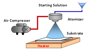
Fig. 1. Schematic diagram of SPD apparatus.
Inorganic and organic metal compounds in solutions are variously used as raw materials for SPD. The principal component and composition of starting solution are held in the deposited film except for easily evaporated additives as it is; namely, this method gives normally the prescribed component and composition of the film.
2. Deposition Process
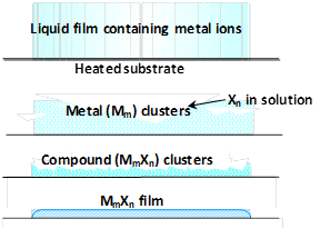
Film deposition from liquid phase occurs according to the following steps, as shown in Fig. 2. ① Innumerable mists from an atomizer wet to make liquid film on the substrate just after sprayed and the boiling temperature of a solvent can be kept until its complete evaporation according to the Gibbs’s Phase Rule, despite the substrate temperature which is set much higher than the boiling temperature of the solvent. ② The temperature of the remained solute increases rapidly to yield metal clusters throughout thermal decomposition and/or chemical reaction. ③ Instantly these metal clusters could be converted to compound clusters by reacting with negative ions existed in the solution. ④ Finally the condensation and cohesion of these compound clusters on the substrate yields solid film immediately.
3. Features
SPD is one of the chemical thin film formation methods and makes dense and even thin films with film thickness 10 nm to 10 µm from solution. Complex compound and solid solution films are also available as non-equilibrium or meta-stable phases according to the control of starting solutions and substrate temperatures. The shape and size of particles in polycrystalline film, the microstructure and texture are controllable by choosing deposition conditions. Further, film thickness increases in proportion to the concentration of starting solution, spray rate and time, and a number of cycles, and is affected by substrate temperature, the vapor pressure of solute, and wetting ability of starting solution. It has been speculated that atomic diffusion or movement occurs to advance the crystallization of fine particles and the densification of texture in film, while the atomizing is stopped for avoiding the reduction of substrate temperature. This stopping could contribute to the quality of the deposited film.
Promising Future Developments
-
Manufacturing and sales of Transparent Conductive Oxide Thin Film (TCO)
We will use the SPD technique to prepare fluorine-doped tin oxide (FTO) and tin-doped indium oxide (ITO) thin films on a glass surface, which have high performance of electrical conductivity and visible light transmittance. These TCOs are applicable to display panels of the cell phones, electromagnetic shielding glass, solar cells and so on.
-
R&D on Dye-sensitized Solar Cell (DSC) and Perovskite Solar Cell (PSC)
DSC consists of two kinds of an electrode; one is a photoelectrode coated with a porous layer of wide band-gap semiconductor and dye. The other is a counter electrode coated with a very thin layer of platinum. The space between these two electrodes is filled with an electrolyte. Without a vacuum system, no hazardous materials, and also with low cost, DSC is attractive as the next-generation solar cell in place of current expensive silicon solar cells. It is possible to save up to more than 50% of the cost by switching to DSC.
-
Instrumentation for solar cell fabrication and power storage process.
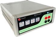
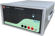
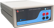
Clean and enormous energy supply is an urgent demand for favorable economic growth all over the world. We would like to construct photovoltaics with DSC/PSC and power storage with a battery/Supercapacitor combined system for the achievement of this request just from now, making the use of our different experiences. Recently, we have initiated the research of PSC processing together with a piezoelectric-inkjet-printing technology, and PV power analyzers with MPPT technique. Nowadays we are in the face to serious problems with global warming and nuclear power generation. We wish to contribute continuously to the development of next-generation solar cell research making a connection with a better solution to these problems through collaboration with highly motivated scientists and engineers.
Papers
- “Large Area Dye-sensitized Solar Cells with Titanium Based Counter Electrode” G. R. A. Kumara, S. Kawasaki, P. V. V. Jayaweera, E. V. A. Premalal, S. Kaneko Thin Solid Films 520, (12), 4119-4121 (2012)
- “Fabrication of Automatic Electrolyte Filling Machine for Dye-Sensitized Solar Cells”
P. V. V. Jayaweera and S. Kaneko Instrumentation Science and Technology 40 (6) 490-503 (2012)
- “Development of Quality FTO Films by Spray Pyrolysis for Dye-sensitized Solar Cell,” Premalal, Edirisinghage VA, Nilupulee Dematage, Shoji Kaneko, and Akinori Konno.Electrochemistry, 80 (2012) 624-28.
- "Preparation of high quality spray-deposited fluorine-doped tin oxide thin films using dilute di(n-butyl)tin(iv) diacetate precursor solutions,” Premalal, E.V.A., Dematage, N., Kaneko, S. and Konno, A. Thin Solid Films, 520 (2012) 6813-17.
- "Ethylene Glycol Assisted Synthesis of Fluorine Doped Tin Oxide Nanorods Using Improved Spray Pyrolysis Deposition Method” Devinda Liyanage, Herath Mudiyanselage Navaratne Bandara, Viraj Jayaweera, and Kenji Murakami. Appl. Phys. Express(6) 085501-04 (2013)
- "Photo Induced Reductive Leaching of Iron from Ilmenite in Hydrochloric Acid Solutions” Jayaweera, P M; Jayaweera, P V V; Jayasundara, U L; Jayaweera, C D; Peiris, G S; Premalal, E V A, Mineral Processing and Extractive Metallurgy, 120, (3), 191-196 (2011)
- "Synthesis of various F-doped tin oxide nanostructures on the glass substrate by the atomized spray pyrolysis deposition for DSSC application (電子デバイス)."Rajapakse, R. M. G., D. Liyanage, P. V. V. Jayaweera, E. V. A. Premalal, V. M. Mohan, H. M. N. Bamdara, Masaru Shimomura, and Kenji Murakami. 電子情報通信学会技術研究報告= IEICE technical report: 信学技報 113, no. 449 (2014): 37-42.
- "Origin of the Hysteresis in I-V Curves for Planar Structure Perovskite Solar Cells Rationalized with a Surface Boundary InducedCapacitance Model" Ludmila Cojocaru, Satoshi Uchida, Piyankarage V. V. Jayaweera, Shoji Kaneko, Jotaro Nakazaki, Takaya Kubo, and Hiroshi Segawa Chemistry Letters 44, (12), 1750-1752 (2015)
- "Electroanalytical investigation of the losses during interfacial charge transport in dye-sensitized solar cell." Yadav, Pankaj, Kavita Pandey, Brijesh Tripathi, P. V. V. Jayaweera, S. Kaneko, and Manoj Kumar. Solar Energy 129 207-216 (2016)
- "Simulation of current–voltage curves for inverted planar structure perovskite solar cells using equivalent circuit model with inductance." Cojocaru, Ludmila, Satoshi Uchida, Piyankarage V. V. Jayaweera, Shoji Kaneko, Yasutake Toyoshima, Jotaro Nakazaki, Takaya Kubo, and Hiroshi Segawa. Applied Physics Express 10, no. 2, 025701 (2017)
- "Reply to comment on Simulation of current--voltage curves for inverted structure perovskite solar cells using equivalent circuit model with inductance" Cojocaru, Ludmila, Satoshi Uchida, Piyankarage V. V. Jayaweera, Shoji Kaneko, Yasutake Toyoshima, Jotaro Nakazaki, Takaya Kubo, and Hiroshi Segawa. Applied Physics Express 10, no. 5, 059102 (2017).
- "Determination of unique power conversion efficiency of solar cell showing hysteresis in the I-V curve under various light intensities" Ludmila Cojocaru, Satoshi Uchida, Koichi Tamaki, Piyankarage V. V. Jayaweera, Shoji Kaneko, Jotaro Nakazaki, Takaya Kubo, Hiroshi Segawa. Scientific Reports, 7, 11790 (2017)
- "Effect of TiO2 surface treatment on the I‐V hysteresis of planar structure perovskite solar cells prepared on rough and flat FTO substrates" Cojocaru, Ludmila, Satoshi Uchida, Piyankarage V. V. Jajaweera, Shoji Kaneko, Haibin Wang, Jotaro Nakazaki, Takaya Kubo, and Hiroshi Segawa. Energy Technology July 14, (2017).
- "Versatile synthesis of fluorine-doped tin (IV) oxide one-dimensional nanostructured thin films". Bandara, Ajith, Kenji Murakami, Rajapakse MG Rajapakse, Piyankarage V. V. Jayaweera, Masaru Shimomura, Herath MN Bandara, D. Liyanage, and Edirisinghege VA Premalal. Thin Solid Films 621, 229-239 (2017)
- "Longitudinal analysis of molecular alteration in serum samples of dextran sodium sulfate-induced colitis mice by using infrared spectroscopy" Unil Perera, Hemendra Ghimire, P. V. V. Jayaweera. Infrared Physics & Technology 97, Pages 33-37 (2019)
- "Recent Progress on Extended Wavelength and Split-Off Band Heterostructure Infrared Detectors"
H. Ghimire, P.V.V. Jayaweera, D. Somvanshi, Y. Lao, A.G.U. Perera. Micromachines, 11(6) 547 (2020)
Patents
-
JP4841574 "Dye-sensitized solar cell module and its fabrication method"
-
JP4945491 "Multilayered electrode and dye-sensitized solar cell with its electrode"
-
JP5227194 "Multilayered electrodes"
-
JP5743591 "Thin-film formation method and apparatus, and dye-sensitized solar cell fabrication process and its production system"
-
JP5963902 "Dye-sensitized solar cell fabrication process and its production system"
-
JP5979656 2 "Ultraviolet irradiation and curing apparatus"
|
|
|
|